- 您现在的位置:买卖IC网 > Sheet目录1242 > SFPA32GBQ1BO8TO-I-QT-223-STD (Swissbit NA Inc)FLASH SSD SMART UDMA 2.5" 32GB
�� �
�
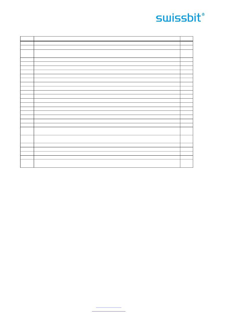
�Table� 23:� Ultra� DMA� Data� Burst� Timing� Descriptions�
�Name� Comment�
�t� 2CYCTYP� Typical� sustained� average� two� cycle� time�
�Notes�
�t� CYC�
�t� 2CYC�
�Cycle time allowing for asymmetry and clock variations (from STROBE edge to STROBE edge)�
�Two� cycle� time� allowing� for� clock� variations� (from� rising� edge� to� next� rising� edge� or� from�
�falling� edge� to� next� falling� edge� of� STROBE)�
�t� DS�
�t� DH�
�t� DVS�
�t� DVH�
�t� CS�
�t� CH�
�t� CVS�
�t� CVH�
�t� ZFS�
�t� DZFS�
�t� FS�
�t� LI�
�t� MLI�
�t� UI�
�t� AZ�
�t� ZAH�
�t� ZAD�
�t� ENV�
�t� RFS�
�t� RP�
�t� IORDYZ�
�t� ZIORDY�
�t� ACK�
�t� SS�
�Data� setup� time� at� recipient� (from� data� valid� until� STROBE� edge)�
�Data� hold� time� at� recipient� (from� STROBE� edge� until� data� may� become� invalid)�
�Data� valid� setup� time� at� sender� (from� data� valid� until� STROBE� edge)�
�Data� valid� hold� time� at� sender� (from� STROBE� edge� until� data� may� become� invalid)�
�CRC� word� setup� time� at� device�
�CRC� word� hold� time� device�
�CRC� word� valid� setup� time� at� host� (from� CRC� valid� until� -DMACK� negation)�
�CRC� word� valid� hold� time� at� sender� (from� -DMACK� negation� until� CRC� may� become� invalid)�
�Time� from� STROBE� output� released-to-driving� until� the� first� transition� of� critical� timing.�
�Time� from� data� output� released-to-driving� until� the� first� transition� of� critical� timing.�
�First� STROBE� time� (for� device� to� first� negate� DSTROBE� from� STOP� during� a� data� in� burst)�
�Limited� interlock� time�
�Interlock� time� with� minimum�
�Unlimited� interlock� time�
�Maximum� time� allowed� for� output� drivers� to� release� (from� asserted� or� negated)�
�Minimum� delay� time� required� for� output�
�drivers� to� assert� or� negate� (from� released)�
�Envelope� time� (from� -DMACK� to� STOP� and� -HDMARDY� during� data� in� burst� initiation� and�
�from� DMACK� to� STOP� during� data� out� burst� initiation)�
�Ready-to-final-STROBE� time� (no� STROBE� edges� shall� be� sent� this� long� after� negation� of�
�-DMARDY)�
�Ready-to-pause� time� (that� recipient� shall� wait� to� pause� after� negating� -DMARDY)�
�Maximum� time� before� releasing� IORDY�
�Minimum� time� before� driving� IORDY�
�Setup� and� hold� times� for� -DMACK� (before� assertion� or� negation)�
�Time� from� STROBE� edge� to� negation� of� DMARQ� or� assertion� of� STOP� (when� sender� terminates�
�2,� 5�
�2,� 5�
�3�
�3�
�2�
�2�
�3�
�3�
�1�
�1�
�1�
�4�
�a� burst)�
�Notes:�
�1.�
�2.�
�The� parameters� t� UI� ,� t� MLI� (in� Figure� 6:� Ultra� DMA� Data-In� Burst� Device� Termination� Timing� and� Figure� 7:�
�Ultra� DMA� Data-In� Burst� Host� Termination� Timing),� and� t� LI� indicate� sender-to-recipient� or� recipient-�
�to-sender� interlocks,� i.e.,� one� agent� (either� sender� or� recipient)� is� waiting� for� the� other� agent� to�
�respond� with� a� signal� before� proceeding.� t� UI� is� an� unlimited� interlock� that� has� no� maximum� time�
�value.� t� MLI� is� a� limited� time-out� that� has� a� defined� minimum.� t� LI� is� a� limited� time-out� that� has� a�
�defined� maximum.�
�80-conductor� cabling� shall� be� required� in� order� to� meet� setup� (t� DS� ,� t� CS� )� and� hold� (t� DH� ,� t� CH� )� times� in�
�modes� greater� than� 2.�
�3.� Timing� for� t� DVS� ,� t� DVH� ,� t� CVS� and� t� CVH� shall� be� met� for� lumped� capacitive� loads� of� 15� and� 40� pF� at� the�
�connector� where� the� Data� and� STROBE� signals� have� the� same� capacitive� load� value.� Due� to�
�reflections� on� the� cable,� these� timing� measurements� are� not� valid� in� a� normally� functioning�
�system.�
�4.� For� all� modes� the� parameter� t� ZIORDY� may� be� greater� than� t� ENV� due� to� the� fact� that� the� host� has� a� pull-�
�up� on� IORDY-� giving� it� a� known� state� when� released.�
�5.� The� parameters� t� DS� ,� and� t� DH� for� mode� 5� are� defined� for� a� recipient� at� the� end� of� the� cable� only� in� a�
�configuration� with� a� single� device� located� at� the� end� of� the� cable.� This� could� result� in� the� minimum�
�values� for� t� DS� and� t� DH� for� mode� 5� at� the� middle� connector� being� 3.0� and� 3.9� ns� respectively.�
�Swissbit� AG�
�Industriestrasse� 4�
�Swissbit� reserves� the� right� to� change� products� or� specifications� without� notice.�
�Revision:� 1.00�
�CH-9552� Bronschhofen�
�Switzerland�
�www.swissbit.com�
�industrial@swissbit.com�
�P-120_data_sheet_PA-QxBO_Rev100.doc�
�Page� 18� of� 76�
�发布紧急采购,3分钟左右您将得到回复。
相关PDF资料
SFPK-SL
CONN SFP CAGE
SFSA16GBV1BR4TO-I-QT-226-STD
FLASH SLC UDMA/MDMA/PIO 16GB
SFSA32GBQ1BR8TO-I-QT-226-STD
FLASH SLC UDMA/MDMA/PIO 32GB
SFSA32GBU1BR4TO-I-NC-216-STD
FLASH X-200M SLC MSATA 32GB
SFSA32GBV1BR4TO-I-NC-216-STD
FLASH X-200S SLC SLIM SATA 32GB
SFSA64GBQ1BR8TO-I-NC-216-STD
FLASH SSD UDMA IND 2.5" 64GB
SFSO4404NR
FEMALE SCREWLOCK 4-40 .197"
SFW22R-1STE1
SFW22R-1STE1-FFC/FPC CONN
相关代理商/技术参数
SFPA32GBQ1BO8TO-I-QT-243-STD
制造商:SWISSBIT NA INC 功能描述:FLASH
SFPA36AT0250
制造商:General Electric Company 功能描述:SFP 3P 600V 250A
SFPA4096Q1BO2TO-C-DT-243-STD
制造商:SWISSBIT NA INC 功能描述:FLASH
SFPA4096Q1BO2TO-I-DT-223-STD
功能描述:FLASH SSD SMART UDMA 2.5" 4GB RoHS:是 类别:计算机,办公室 - 元件,配件 >> 固态硬盘驱动器 系列:P-120 标准包装:1 系列:- 存储容量:64GB 存储器类型:闪存 - NAND 其它名称:VL 64 GB SSHD KITVL64GBSSHDKIT
SFPA4096Q1BO2TO-I-DT-243-STD
制造商:SWISSBIT NA INC 功能描述:FLASH
SFPA-53
制造商:未知厂家 制造商全称:未知厂家 功能描述:Schottky Barrier Diodes
SFPA-63
制造商:SANKEN 制造商全称:Sanken electric 功能描述:Schottky Barrier Diodes (Surface Mount) 30V
SFPA-73
制造商:未知厂家 制造商全称:未知厂家 功能描述:Schottky Barrier Diodes